

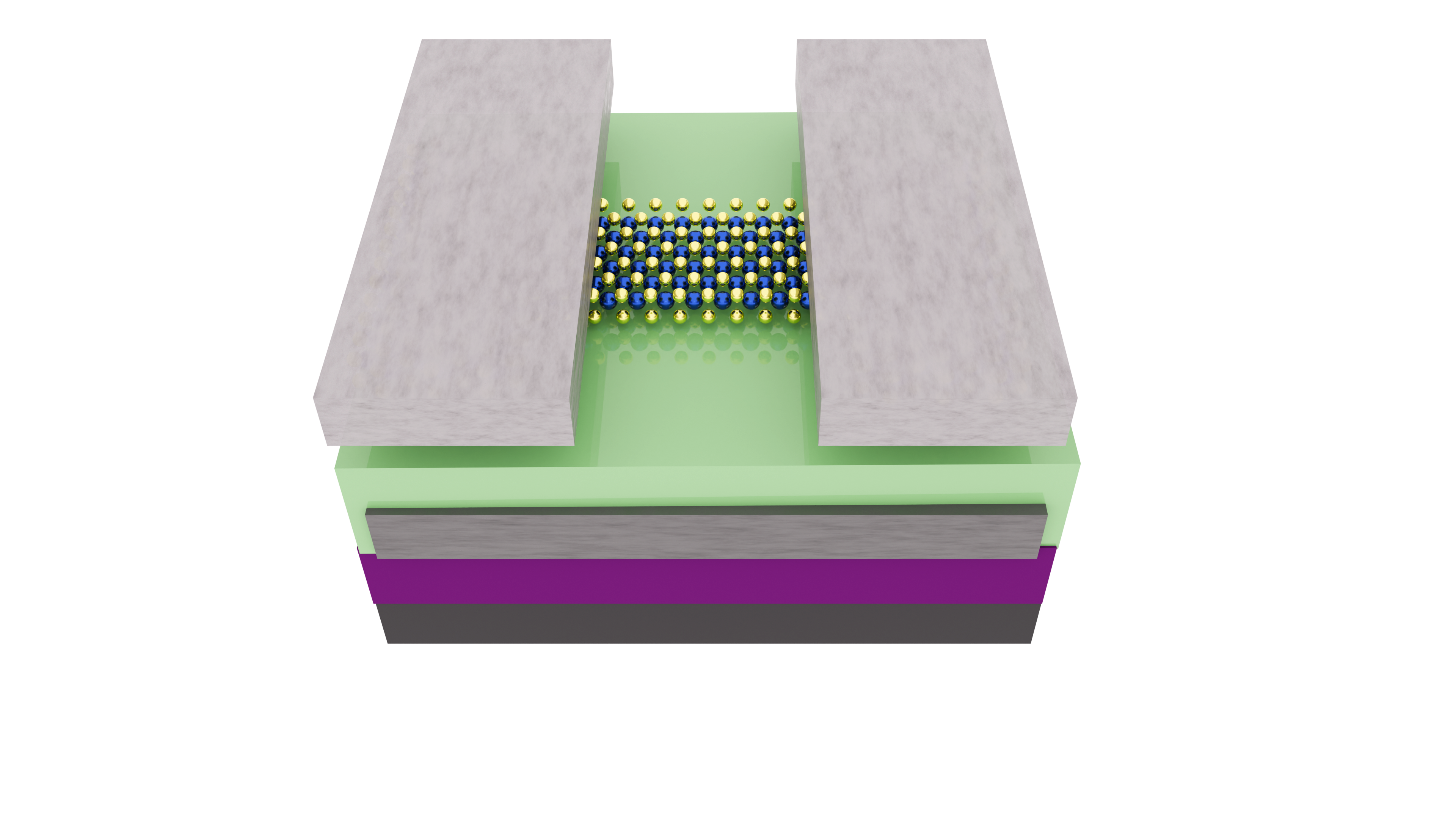
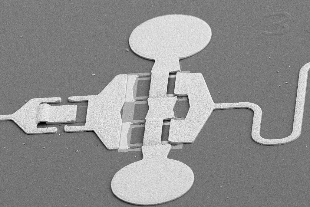
Our main project is to study transistors based on atomically thin 2D semiconductors (transition metal dichalcogenides, TMDs), with a central question in mind: can these materials realistically complement silicon in future electronics? Through advanced cleanroom fabrication, state-of-the-art electrical characterization, and device simulations, we explore how 2D semiconductor transistors behave when pushed to their limits. Our focus is on the device physics and materials science that matter for memory technologies, from flash, DRAM, and SRAM to emerging concepts, using 2D semiconductors grown and integrated in ways that resemble how tomorrow’s chips may be built.
In parallel with our 2D semiconductor work, we collaborate with Niklas Rorsman’s group on gallium nitride (GaN) transistors for high-frequency and high-power electronics. GaN’s wide bandgap and high mobility make it central to future wireless communication systems and power converters. Chalmers is part of the WBG Pilot Line, a Europe-wide effort on the development and pilot production of next-generation wide bandgap device technologies.